Просмотр новости
Найдите то, что Вас интересует
 Спутники
 РН
РН SpaceX
 Роскосмос
 NASA
NASA
СпутникиРНSpaceXРоскосмосNASAMobilint is preparing to begin mass production of its second-generation neural processing unit (NPU), REGULUS, by the end of this year. The company recently delivered customer samples (CS) to clients, marking the start of full-scale product qualification.Dongjoo Shin, chief executive officer of Mobi
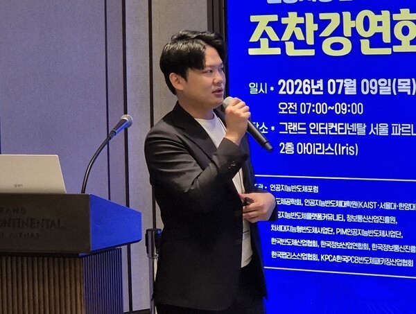
Mobilint is preparing to begin mass production of its second-generation neural processing unit (NPU), REGULUS, by the end of this year. The company recently delivered customer samples (CS) to clients, marking the start of full-scale product qualification.
Dongjoo Shin, chief executive officer of Mobilint, said at the AI Semiconductor Forum breakfast seminar in Seoul on July 9 that REGULUS customer samples are currently being sold commercially and that reliability verification with QRT has been completed.
"Although mass production has been delayed by three to four years compared with overseas competitors, the timing now aligns with the emergence of the physical AI market where the chip will be deployed," Shin said.
Around 90 companies are currently evaluating Mobilint's products, including REGULUS, up from about 70 at the beginning of the year. Potential customers include LG Electronics, POSCO DX, Doosan Robotics, Kolon Benit, LOTTE Innovate, Shinsegae I&C, Daedong and Intellivix.
REGULUS is a 17 mm × 17 mm system-on-chip (SoC) integrating a central processing unit (CPU), video codec, NPU cores, an image signal processor (ISP) and scratchpad memory (SPM) intellectual property (IP). The chip supports Ethernet and USB interfaces, uses LPDDR4X memory and is manufactured on TSMC's 12-nanometer process.
The processor is designed for applications including smart cameras, AI kiosks, industrial robots and agricultural machinery. Shin said the company has received growing inquiries from customers seeking alternatives to Chinese chips supplied by vendors such as Rockchip.
Mobilint is targeting both on-premises and on-device AI systems, enabling edge AI inference without relying on cloud connectivity. The company's principal competitors in the global edge AI chip market include NVIDIA's Jetson platform, Qualcomm and Hailo.
Shin said Mobilint's chips deliver significant efficiency advantages over competing products.
"Edge AI requires high performance, competitive pricing and power efficiency," he said. "Our chips can reduce customers' capital expenditure (CAPEX) by half, lower operating costs by three to four times and improve power efficiency by five times compared with competing solutions." He added that edge computing offers lower latency, stronger communications security and higher energy efficiency than cloud-based computing.
Software compatibility is another key differentiator, according to Shin.
"Without broad compatibility, it is impossible to enter the market," he said.
Mobilint's software development kit (SDK) supports 400 AI models across large language models (LLMs), vision-language models (VLMs) and vision-language-action (VLA) models in commercial production environments. Shin said no other global edge AI NPU vendor currently supports VLA models, describing the capability as Mobilint's unique competitive advantage.
The company has also begun developing a successor to REGULUS using a chiplet-based architecture manufactured on a 4-nanometer process. Shin said developing and commercializing a 4-nanometer chip requires at least 100 billion won. Mobilint recently raised 70 billion won in a Series C funding round. The next-generation chip will be fabricated using Samsung Electronics' 4-nanometer process, while SEMIFIVE will serve as the design house.
Chiplet technology packages multiple smaller chips into a single processor rather than relying on one large monolithic die. As system-on-chip functionality continues to expand, larger chip sizes can reduce manufacturing yields. A chiplet architecture distributes key functions across multiple dies, improving yield while providing greater scalability.